Click anywhere to close
This is part two of my two part series on how to build a simple motherboard for your electronics project. Following the steps in this guide is how I designed basically all of my PCBs, including the the one for my Smart Thermostat.
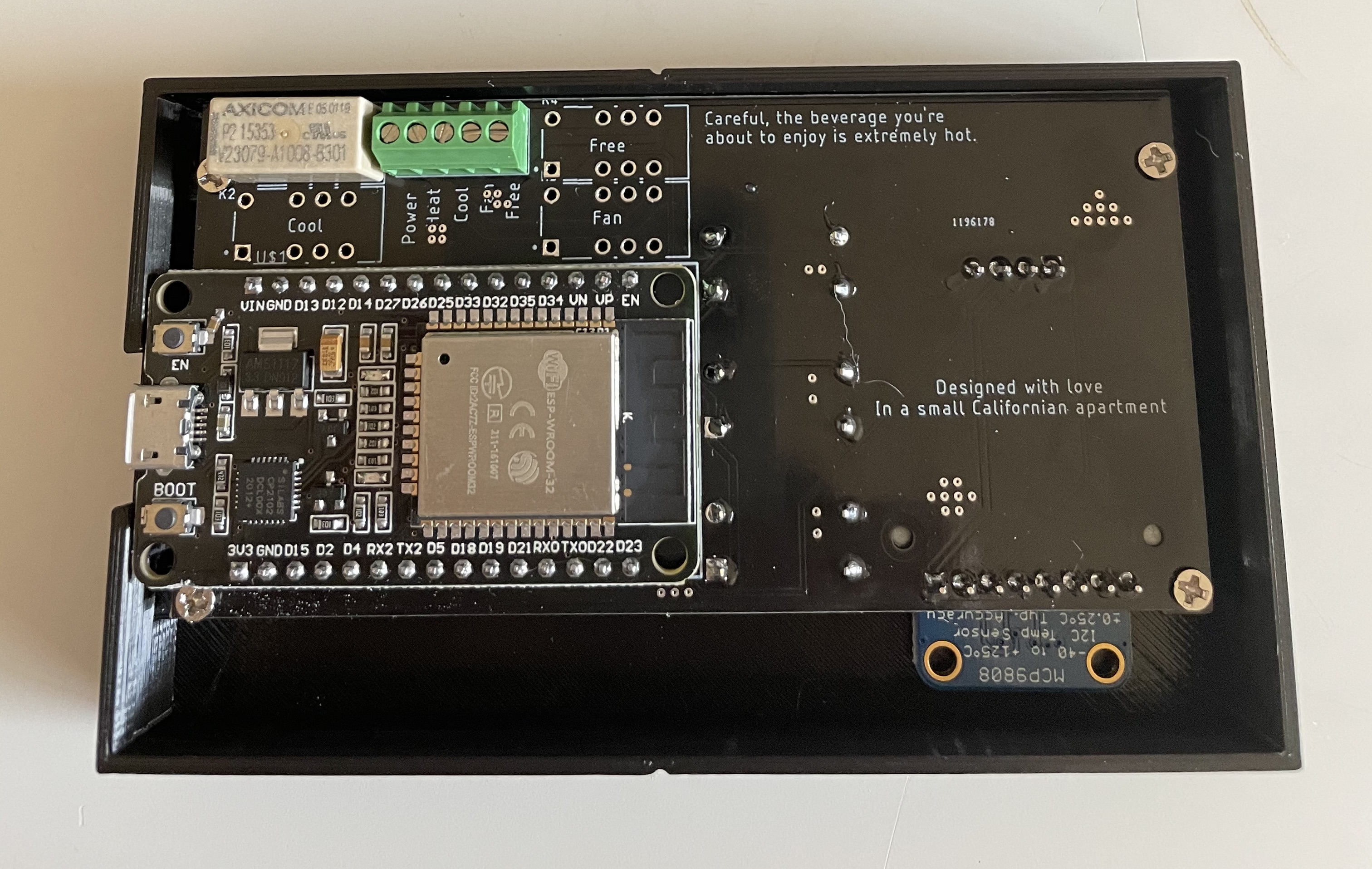
Here is an example of the motherboard I designed for my Thermostat project
You can find Part One here, where I cover the first steps of building a board, Components & Schematic.
If you have any questions at all please feel free to reach out to me directly. If you want to stay up to date on my projects or see other guides like this one, feel free to subscribe to my email list or RSS feed. My next post will be about my experience designing and building a custom guitar from scratch.
Once the schematic is complete, or mostly complete, we can move over to the board layout and start physically designing our PCB.
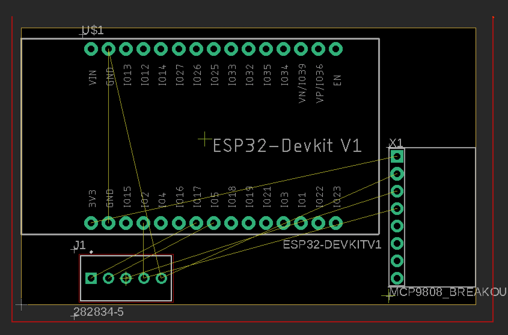
When you first open your layout, you will be presented with something like this
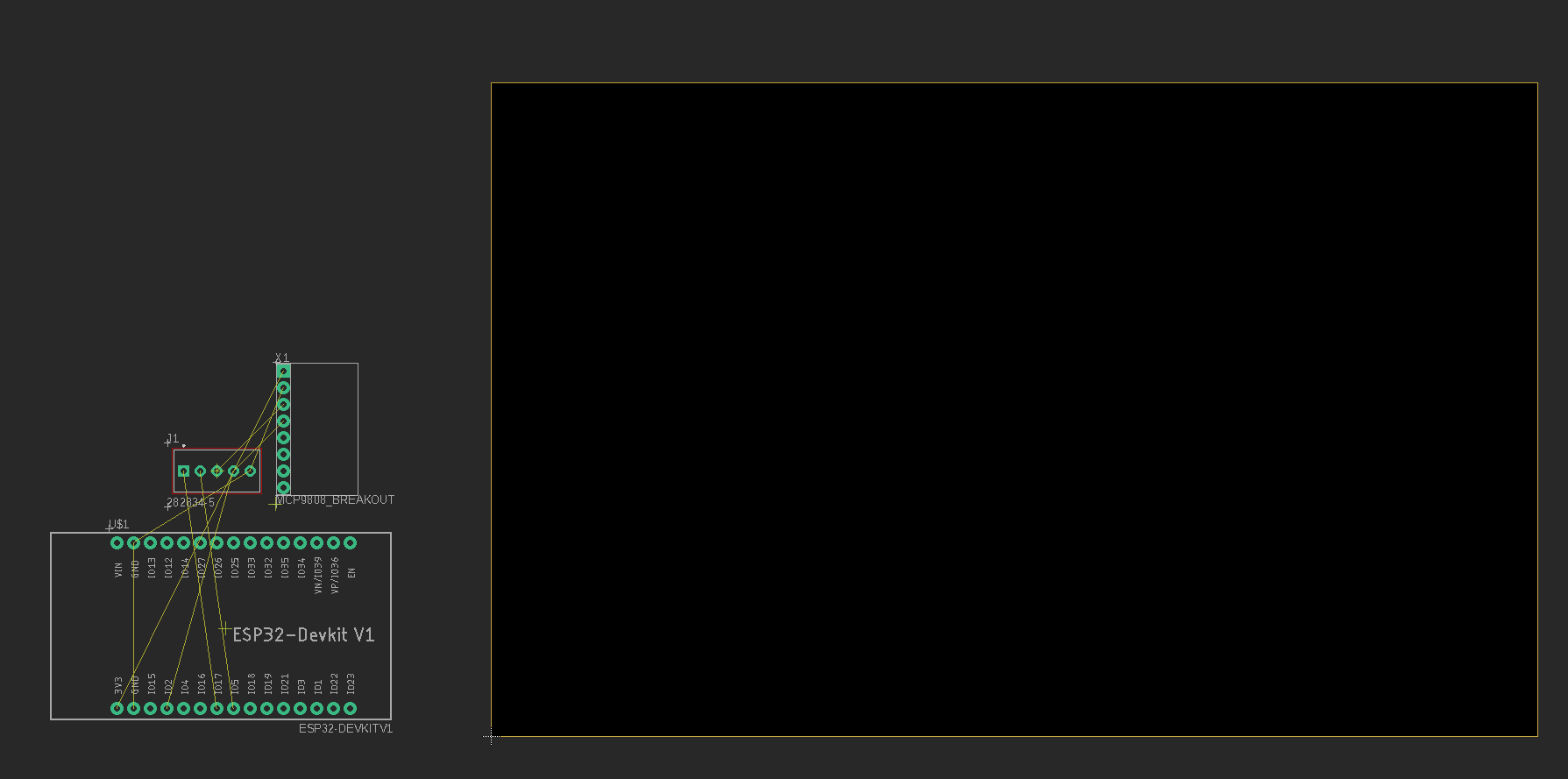
There’s a lot of stuff going on on this screen, here’s a quick list of what’s on screen:
PCB manufacturing has a bunch of physical constraints that limit various parts of your layout. These are things like minimum size of a trace or minimum distance between traces. A lot of the time they will provide a list of constraints, so check your manufacturer’s website for some instructions. In this guide I will use safe rules that have worked for every manufacturer I have ever used.
The most important setting is your trace width and clearance, these are controlled in Eagle using “Net Classes”. You should set the defaults to good values before you begin layout routing to simplify things down the line.
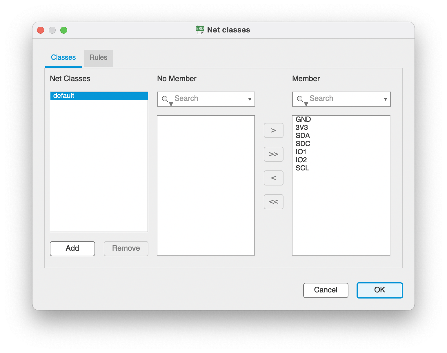
Select the “Net Classes…” option from the Edit menu in Eagle. On the left menu you will see a list of all of your net classes, and on the right you will see what nets are part of that net class. Click the “Add” button and add a “power” net class. Add all of your power lines (3V3, …) to this net class, we will set the rules for this class to use slightly wider traces for safety.
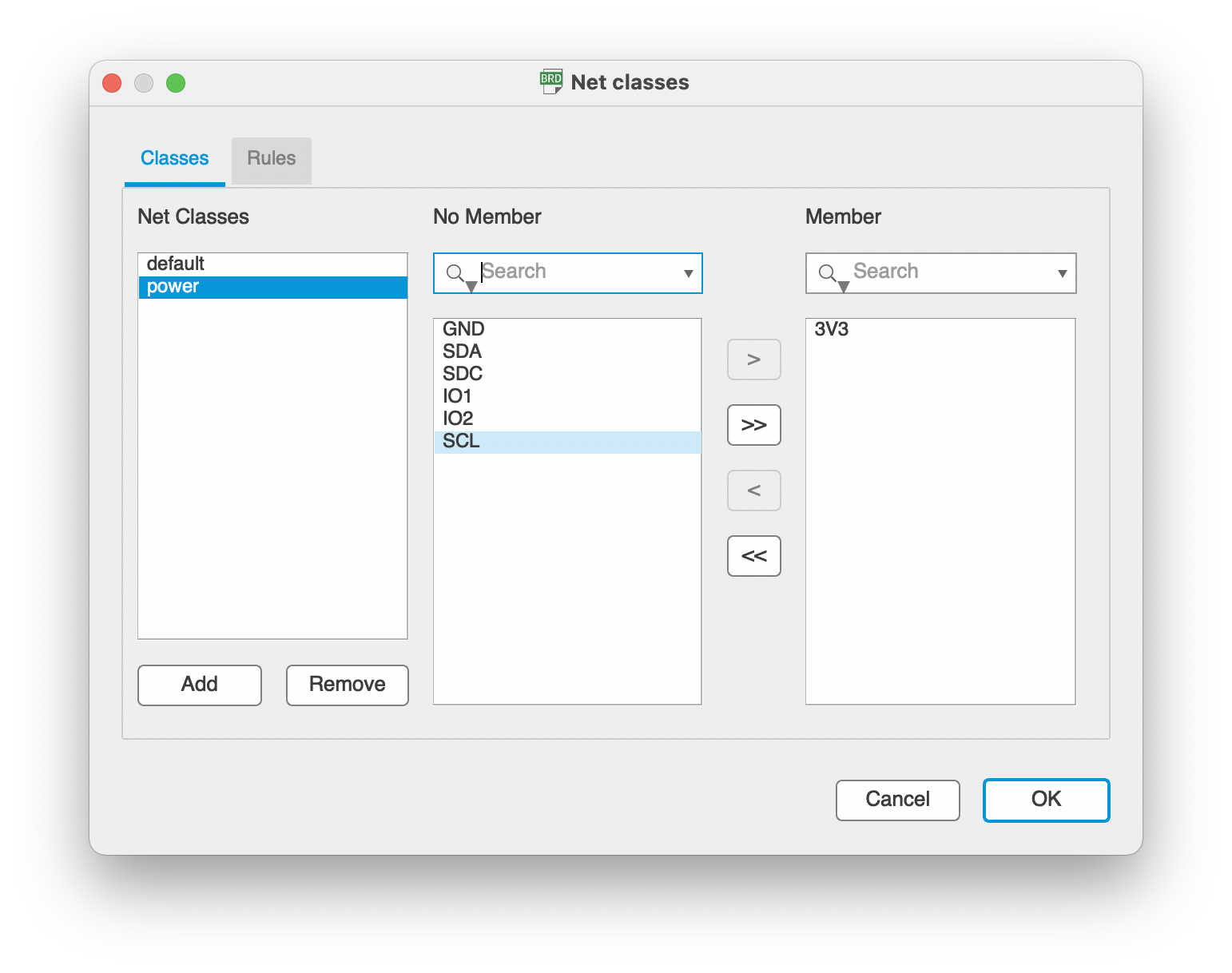
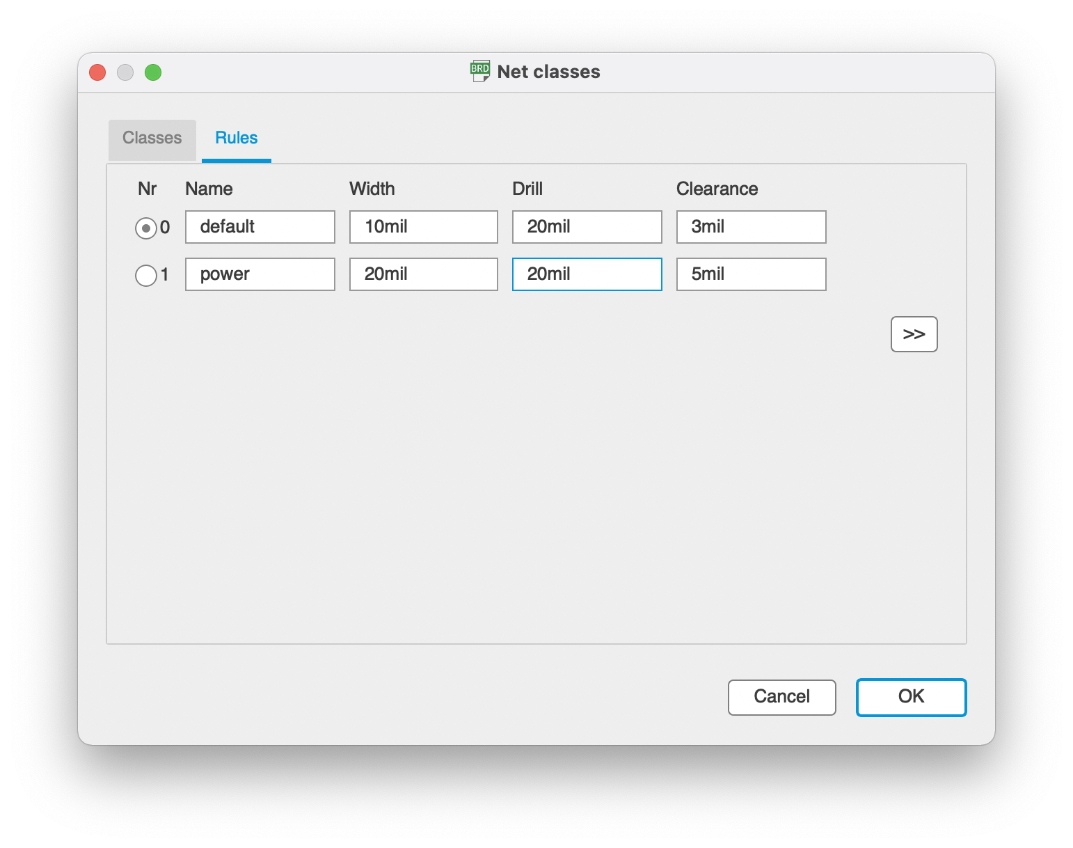
Select the rules tab, and then set your rules to what I have in the image above. Generally I use ~10mil traces for signal and ~20mil traces for power. These can vary, and will depend a lot on your manufacturer and your application. I have found these defaults to be fine for most common applications. I have also set the clearances to 3mil and 5mil, these are chosen to be much higher than the manufacturer minimum, feel free to modify them as you see fit but make sure you stay within your manufacturers constraints.
Once you have set up your net classes click OK to continue to the Placement and Routing portion of our tour.
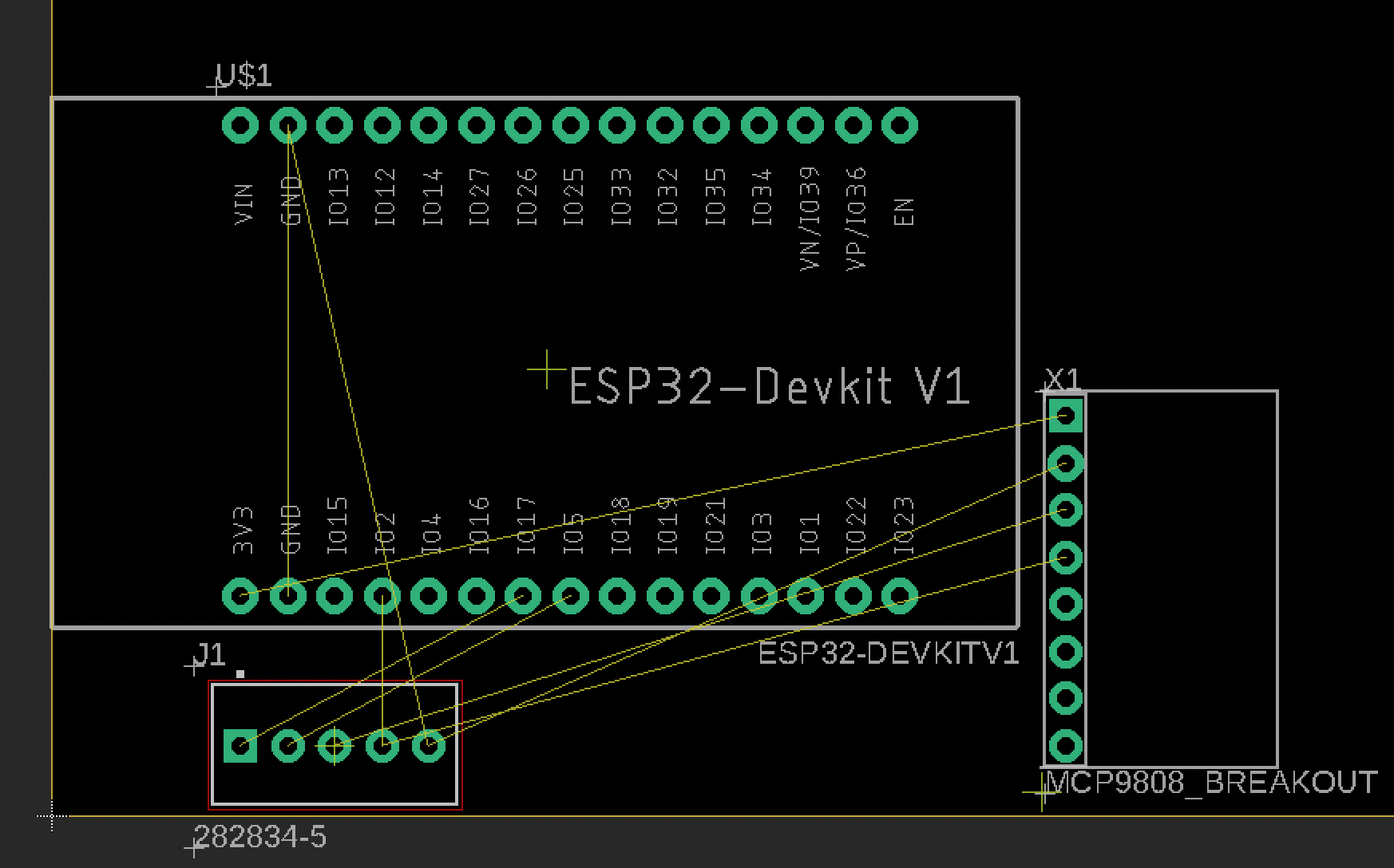
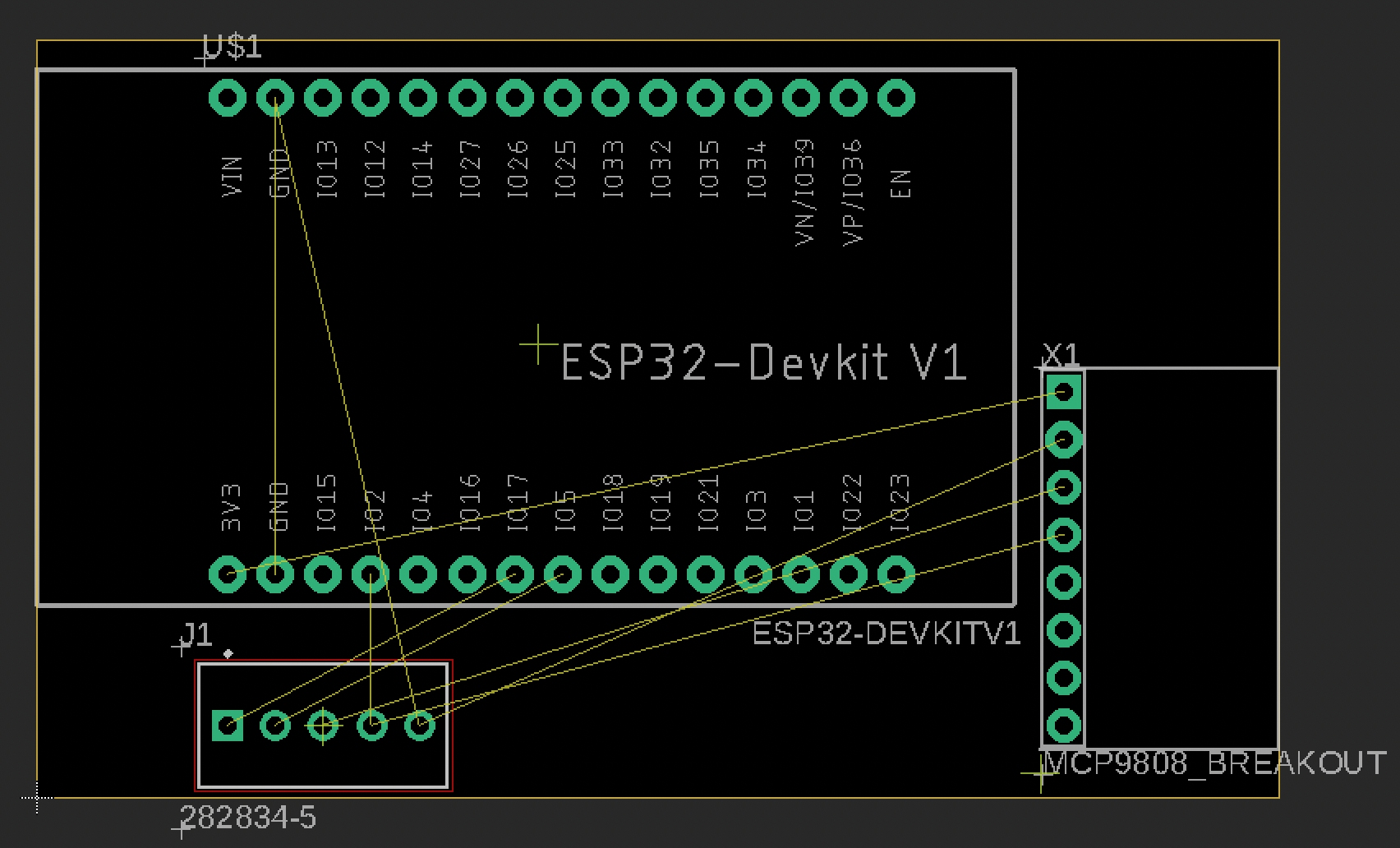
First step is to place all of your components on to the PCB. Generally I start with any physical constraints I have, in this case I want the ESP32 to be on the edge of the board so I can plug in the USB, so I will place that first. I will then place the other components.
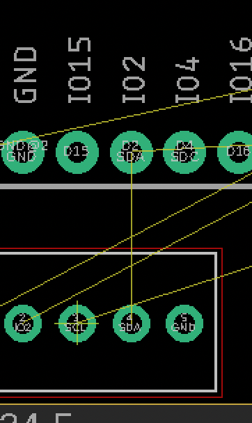
A good tip for simplifying things down the road is to try to avoid the yellow air wires crossing whenever possible. Generally the simpler the air wires, the simpler trace routing will be.
So start with the largest component and work your way to the smallest component. Your goal here is to keep the air-wires as clean as possible while utilizing as little space as you can. If you have GPIO air-wires that you can’t uncross it’s often a good idea to go back into the schematic file and swap the pins. The simpler you can make your layout the easier the next step will be.
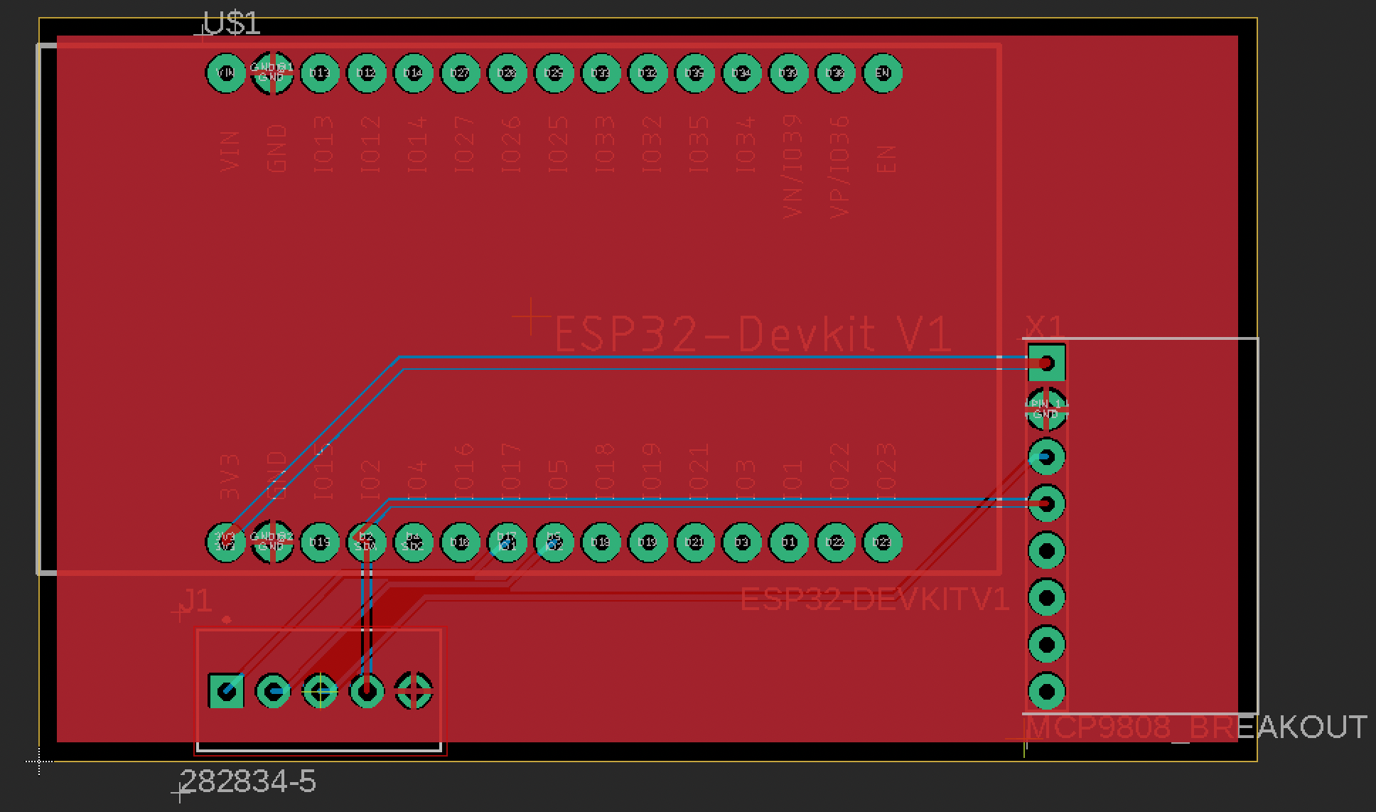
Here is how my example ended up when I was finished layout:
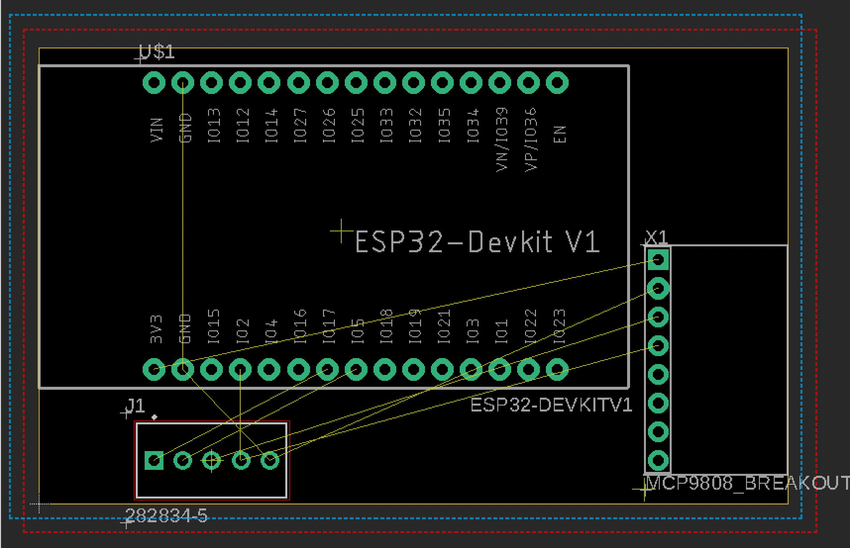
Once you get a majority of your components placed within the outline, you can resize your outline to fit your components. This step is important, if you don’t resize your outline your boards will come back huge.
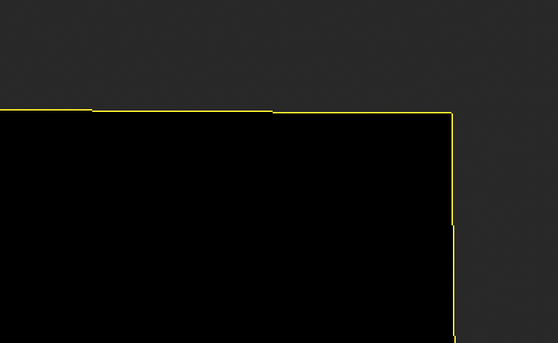
You can resize the outline by clicking on the yellow line, this will begin moving it, moving your cursor to your target position, and clicking again to stop moving. In my example I shrunk the outline to just contain the parts.
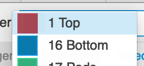
PCBs can contain many layers of routing. A layer is a single plane on which you can draw traces. Traces on two different layers will not collide with each other, allowing you to cross traces. The standard (and cheapest) option is to use a Two layer board. On a two layer board you will have traces on both the Top and Bottom of the board. By default your PCB Layout in Eagle should be two layers. You can view the layers by clicking the “Layers” dropdown in the top left.
If you can not solve (connect all your nets) your layout cleanly with two layers, consider re-arranging the parts and pins, as it’s much cheaper than adding more layers to your board.
Before we route all of our signal traces, we should draw our ground planes. In most scenarios we will use traces (lines) to connect the power and signal nets together, however we will use planes to connect the ground nets. Ground planes are designed to reduce noise in your PCB, and also simplify routing (since almost every component needs to connect to ground, it makes it easier to do them all in bulk).
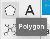
Creating a ground plane in Eagle is easy. Select the layer you want to draw on using the Layer dropdown, choose the polygon tool from the left and draw a box around your board. Draw the ground plan larger than your board outline to ensure that the plane covers your entire board.
Do this once for each layer on your board (Top and Bottom). You can switch layers using the Layer dropdown. When you are finished you should have two rectangles, one red and one blue, around the outside of your board.
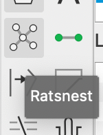
Just drawing the ground plane will not “Pour” the ground plane. If you want to see what traces the ground plane will draw, press the Ratsnest button.
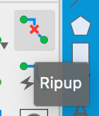
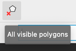
You can undo the pour by selecting the Ripup tool from the left pane, and then selecting “all visible polygons” from the top menu. You will want to do this before continuing as it’s difficult to route while the ground planes are visible.
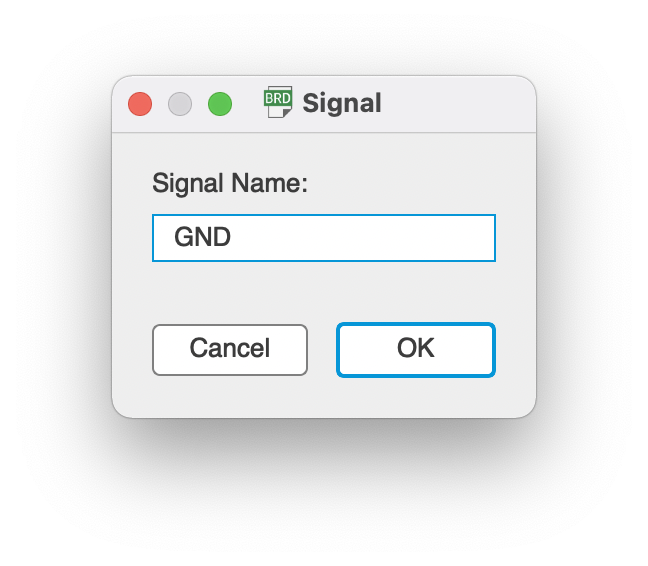
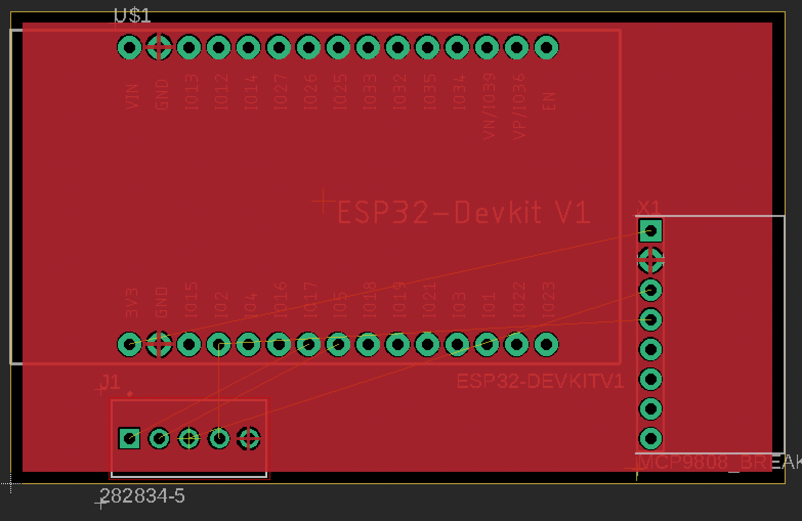
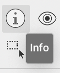
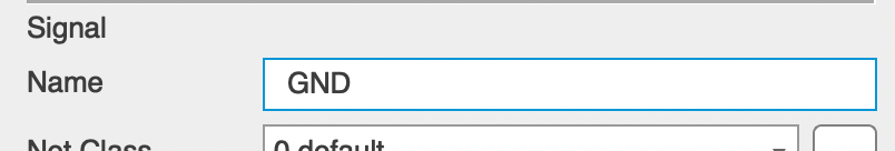
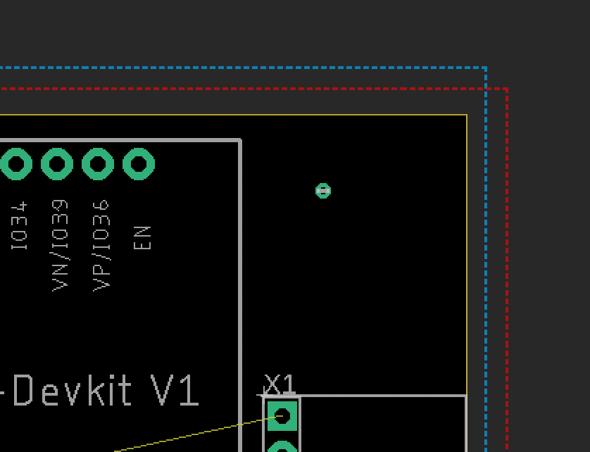
Note how there are connections to your GND pins (they look like little pluses on those pins), but no other pins. If you do not see connections to your ground pins, rip up the ground planes, select the “Info” tool from the left menu, click on the outline of your plane, and make sure the signal name is set to GND.

The last thing we need to do before moving on to signal routing, is add some vias between our two ground planes. As it stands our two planes are very poorly connected (only connected via the through hole pins). We add some vias to increase their connectivity, and make routing a bit simpler later.
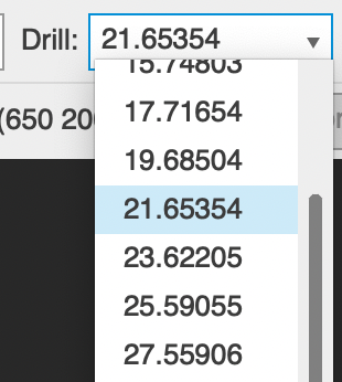
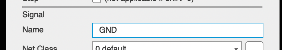
To add a via select the via tool, change the drill size to something around 20, and click to add a single via to your PCB. Important after adding a via to your board, select the Info tool from the left, click on your via, and change the Signal Name to GND, otherwise it will not connect anything!
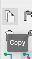
You’ll want to place these vias out of the way, probably around the edge of your parts. We want at least a handful of vias on our board. After creating the first one, it’s easiest to use the Copy tool to create a bunch more, this allow you to skip the Info → Signal Name step on every via.
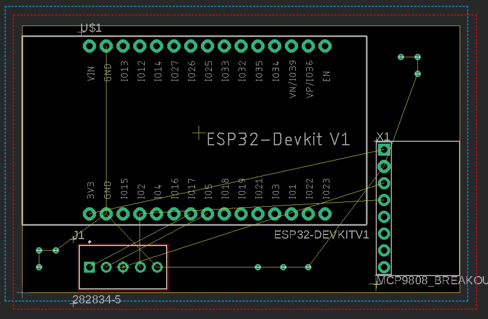
Here you can see my finished board with 9 ground vias. Feel free to add as many as you’d like, just make sure you have them in a bunch of places to simplify routing later. Before you continue, use the Ratsnest button to pour your ground planes and make sure that the vias are touching the planes.
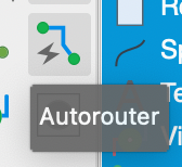
Eagle provides a great tool for simple PCBs like this, known as the auto router. For most simple projects this will provide a reasonable solution to routing and is the easiest way to get your board out the door.
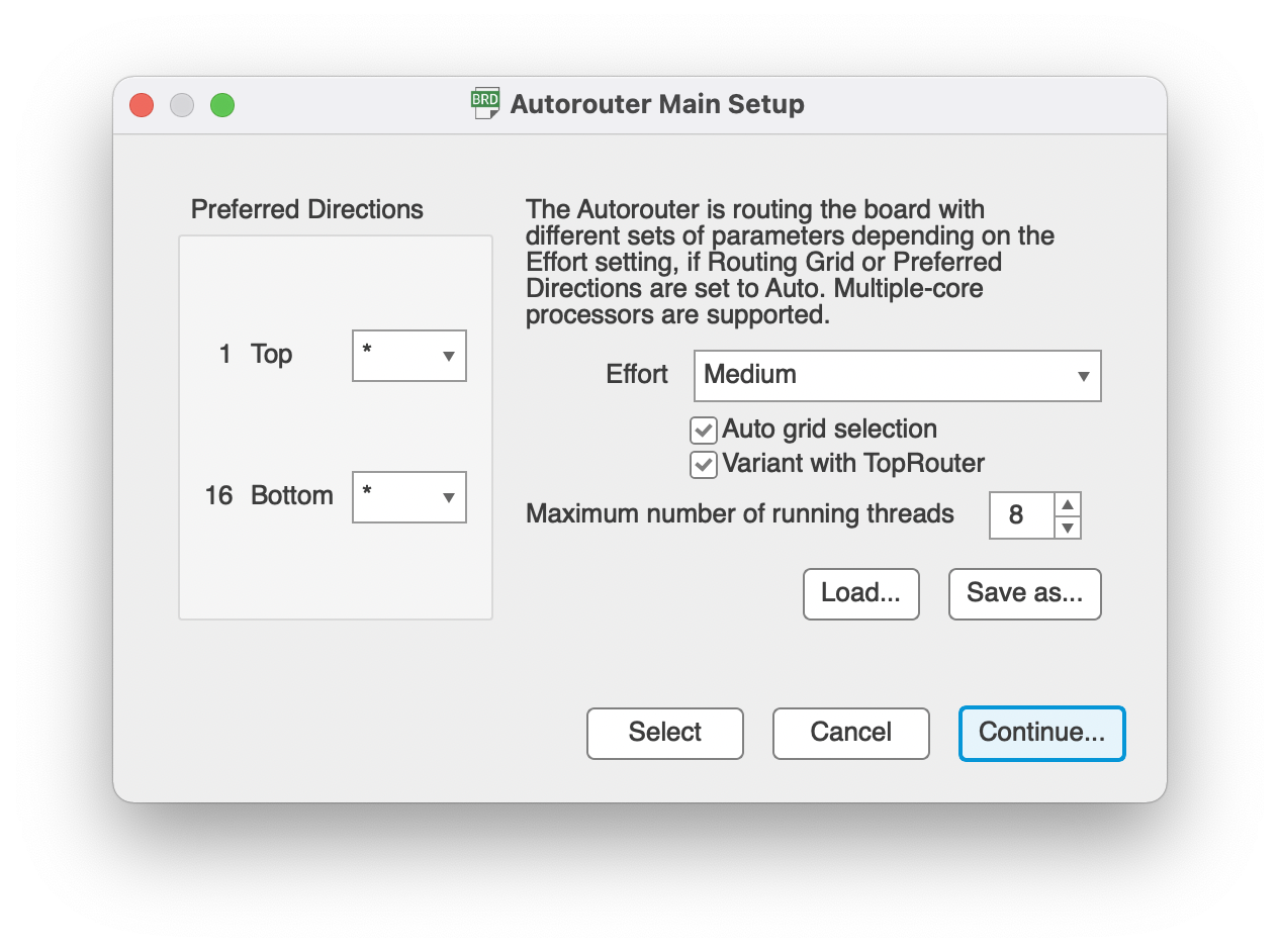
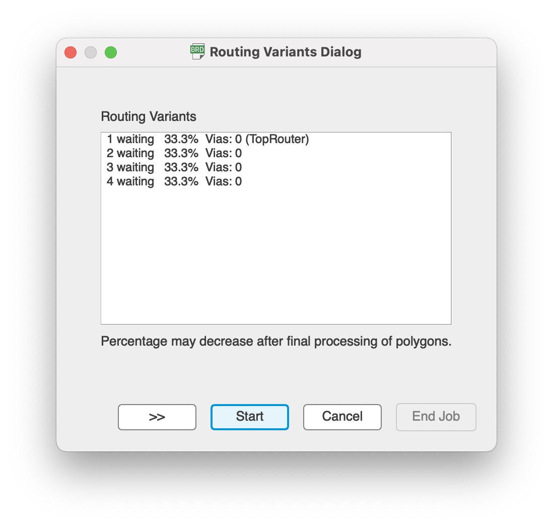
To start the autorouter, ripup your ground planes (instruction above), choose Autorouter from the left menu, click Continue on the prompt, and then click Start. Generally I will leave the settings at default, if you aren’t getting good results you can change the Effort to High which can help.
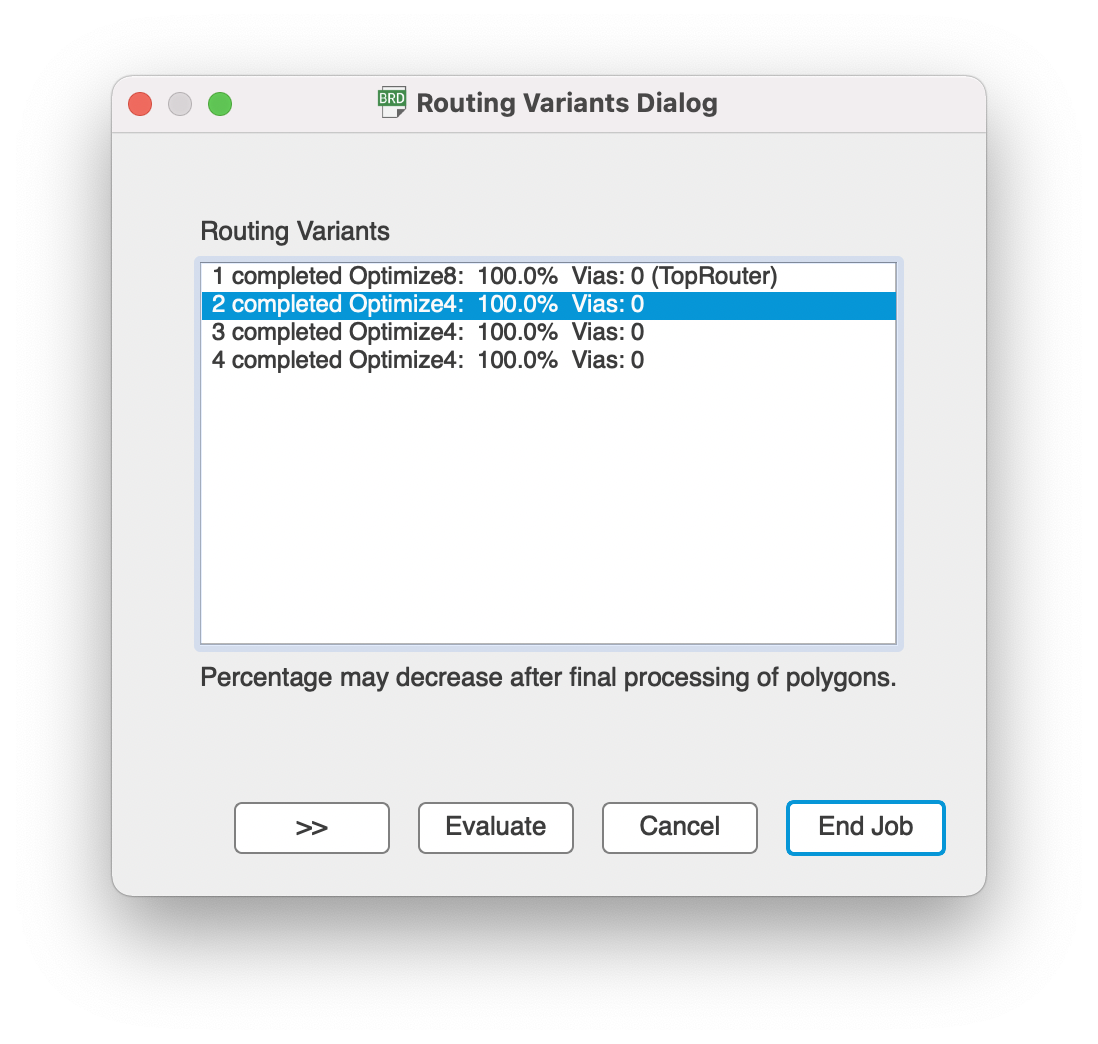
Once all of the variants have completed, you can click through the options and see how they look on your board. In general I try to optimize for the fewest “Vias” although this is not a hard and fast rule. If none of your variants are able to complete, that normally means your layout is not solvable (at least in a simple way) and you may want to consider re-organizing your layout.
To finish, select the variant you prefer, and hit End Job. You will need to ripup and re-pour your ground planes after selecting your route. If you are satisfied with your layout feel free to go on to section 5 about exporting and order. In the next section I will cover the basics of manual routing but you often won’t need them for simple boards.
A lot of EE professionals will tell you to never trust the auto-router. In general the auto-router is a great tool to speed up simple projects, but it can definitely make mistakes and knowing how to route yourself is important.
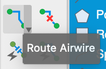
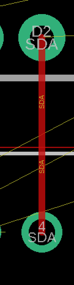
In general your goal in routing is to connect all of the yellow “Air Wires” using traces. In practice this boils down to a core loop of: Select the Layer you want to route on, select the Route Airwire tool, choose a pin, draw trace to another pin, select the other pin. You do this over and over until you have a completed design.
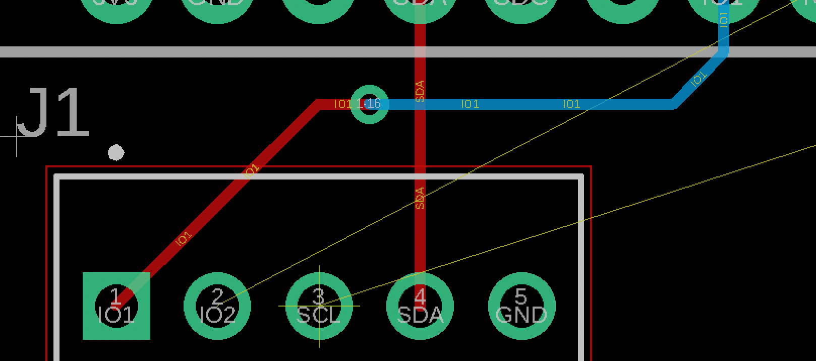
If at any point you need to cross two traces, you can use a Via. A via will connect two layers together. The manufacturer will drill a hole in your board and plate the via with metal to connect the two layers together, allowing you to route traces.
Placing a via is very easy. While you are actively routing, change layers using the Layers dropdown on the top left, and it will automatically give you a via at the end of your trace. Clicking will swap layers and allow you to continue routing on the other side of the board.
Once you have connected every trace (removing all yellow air-wires) continue to the next step.
Now we have completed our board, let’s move on to board validation, exporting and ordering.
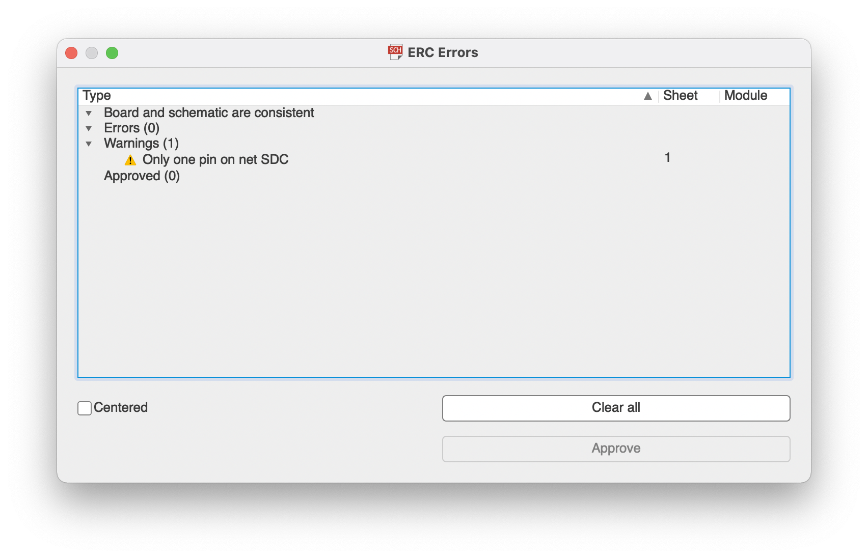
Eagle provides two great automatic checkers to help you avoid problems with your board. These are called ERC “Electrical Rule Check” and DRC “Design Rule Check”. These dialogue can be opened from the tool menu on the bottom.
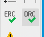
ERC will warn you about issues with your schematic. You can see below it is warning me that I only have one pin on my SDC net. In general you should have No Errors or Warnings before continuing. If you truly believe something is fine, click “Approve” to ignore it.
DRC will check your layout for any errors. This is where you can load your design rules in from your manufacturer. I generally don’t bother as the default rules have always worked fine for me.
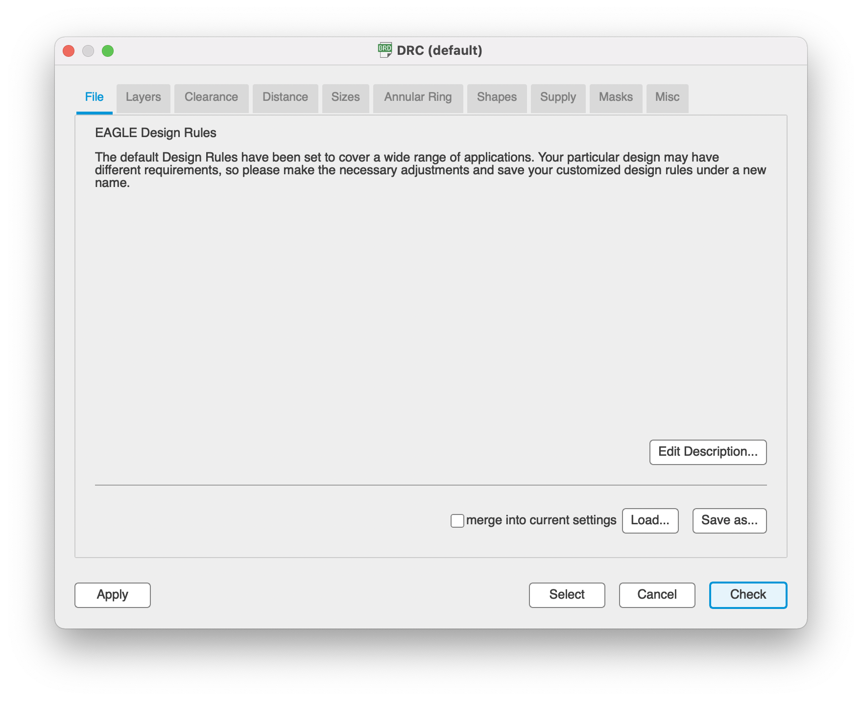
If everything is fine when you press “Check” the menu will disappear, but on the bottom left you will see “No DRC Errors”

Once you sort out any errors with ERC/DRC, move on to manual checking and exporting.
It is very very easy to make a mistake while designing and laying out you board. I always try to take a break and come back to the board with a fresh brain in order to be extra sure there aren’t mistakes in my layout. If you have a friend who knows this stuff it’s a great idea to ask them to review for you as well.
Things to check (that I have definitely forgotten to check before)
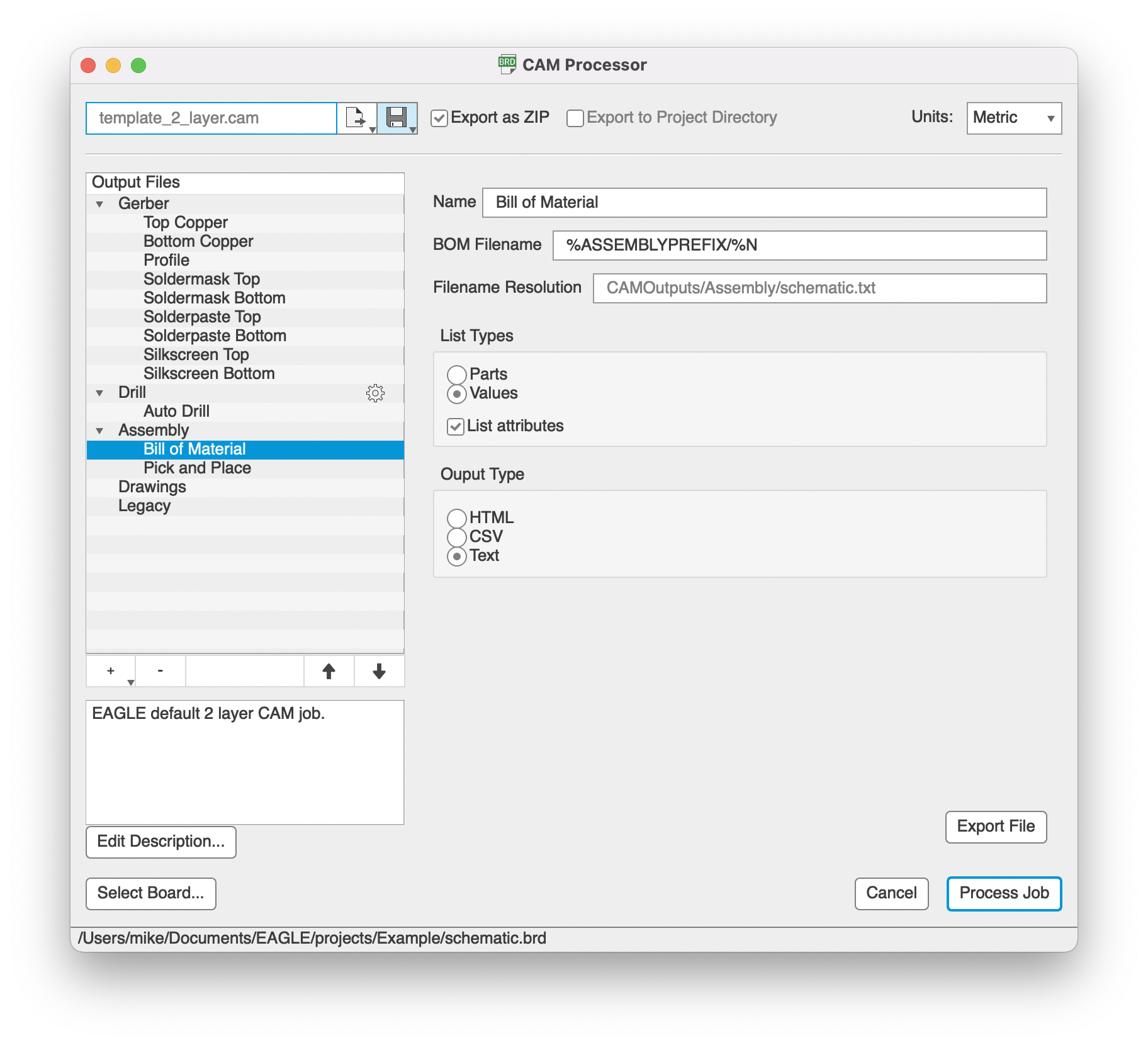
Once you have completed your validation you can export it for uploading to the manufacturer. To do this select Manufacturing from the right side, and click “Cam…”. This will bring up the CAM dialogue.
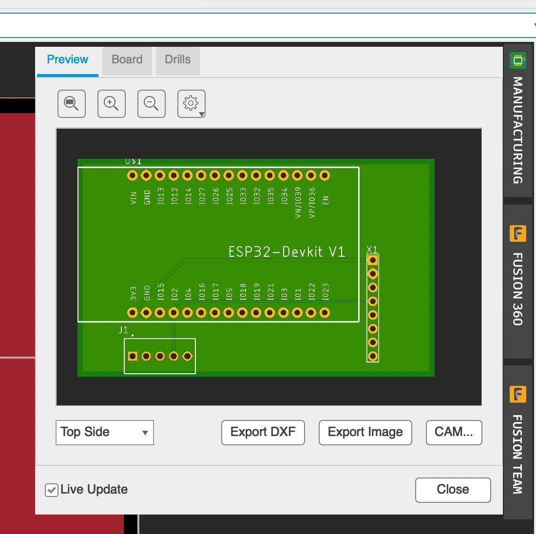
On the CAM… dialogue you shouldn’t need to modify any of the settings, just select “Export as Zip” from the top and then Process Job from the bottom right. This will create a zip file that you can upload to your PCB manufacturer. Save this somewhere you can find it for the next step.
Now comes the fun part, ordering the PCBs. There are a ton of cheap board fabs out there so it’s up to you which to use, they all work basically the same way: First you upload your board, then they review and create the PCBs, then you get your PCBs in about a week.
My fab of choice is Seeedstudios Fusion PCB. I have found their turnaround time to be great, and their prices low. There are definitely others out there: dirtypcb and jlcpcb are also great choices.
This guide will use seeed, to buy board from them use this link
On Seeed it’s extremely easy to order boards. Click the Add Gerber Files and upload that Zip archive we made in the previous step. Change the PCB dimensions to match the outline size you made earlier (you can use the Info tool in the layout to find the exact size). Don’t worry about getting the dimensions exact as they will use the gerber files to get the exactly right size
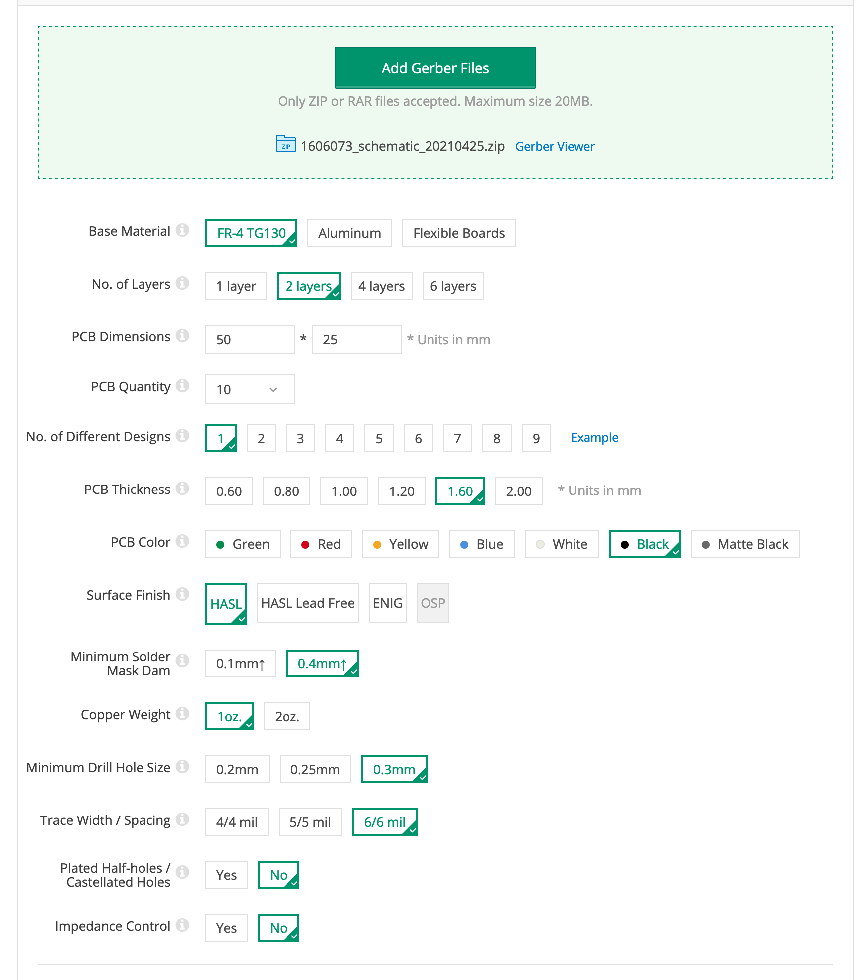
Leaving most of the settings on default is almost always fine, I normally change my PCB color to something cooler than Green, but that’s up to you. When you are finished hit “Add to Cart” and buy your PCBs!
Generally you can get 10 PCBs for about $20 ($5 + the cost of shipping from China). I suggest starting pretty small and then buying more after you validate, from my experience, there is a 99% chance you will want to make modifications to this first design.
Congratulations. You just made your first PCB. Please reach out to let me know how it went, I am always happy to answer any questions or chat projects. mdl0394@gmail.com