Click anywhere to close
After the prototyping phase of any electronics project, I like to make a "Motherboard" PCB. For this phase I will continue to use breakout boards for all of the individual components, but link them together using a PCB. This allows the PCB design to stay simple and flexible, and makes them easy to hand manufacture them in my workshop. This is a great setup if you want to do a small (10ish) beta run of your project before designing a full product. I have shipped many hardware products using this stage, it's a great way to validate your MVP before putting money into tooling and CM bring up.
This tutorial will walk through the process that I follow to create a motherboard. The intended audience is someone who has already wired up a prototype on a breadboard, and wants to get started bundling them together into a motherboard. This will be the guide I wish existed when I got started doing this.
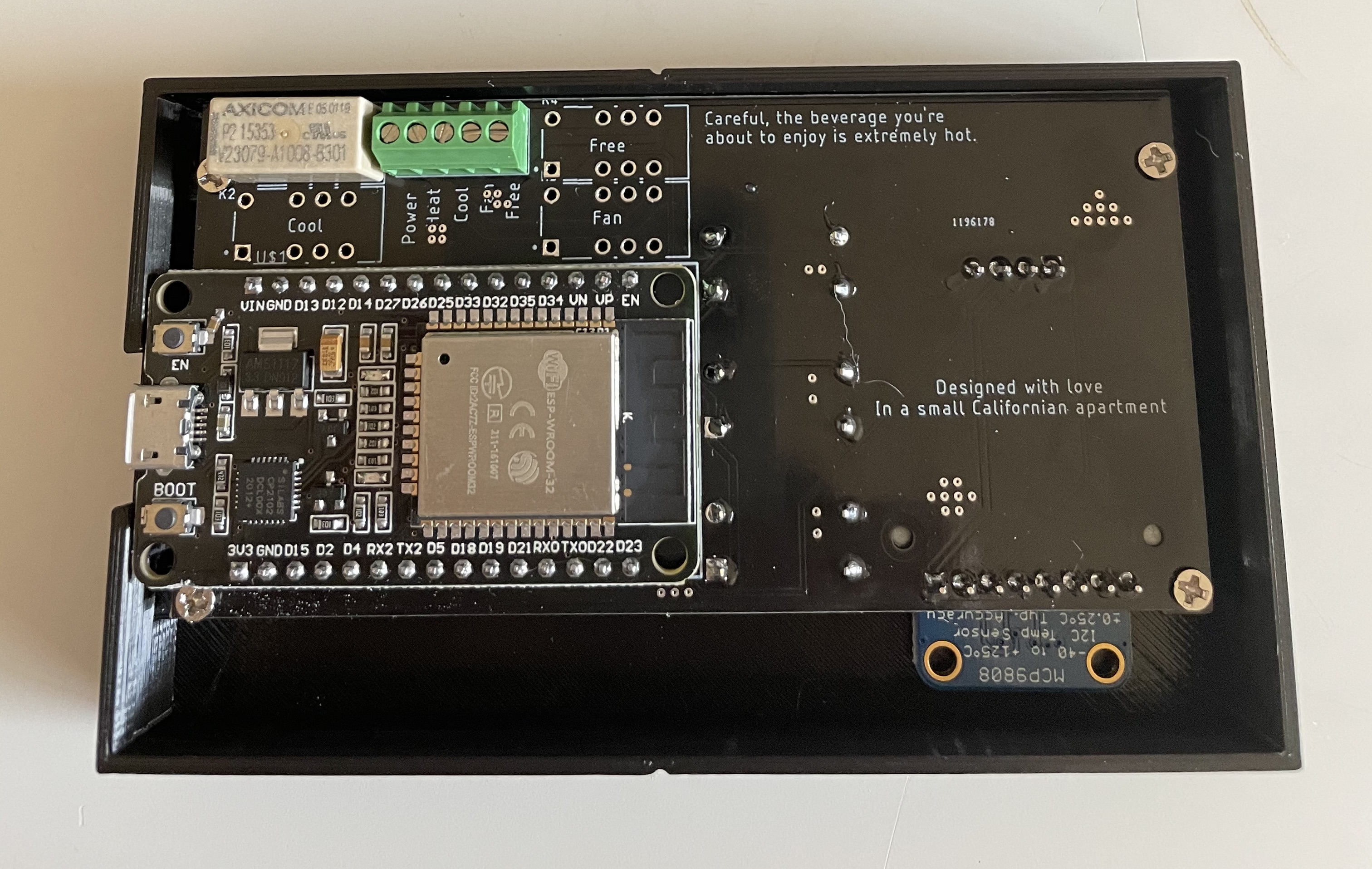
Here is an example of the motherboard I designed for my Thermostat project
This is just the process I figured out for myself, it's by no means perfect. If you have any feedback or questions about any of this stuff, want a PCB design for your project, or just want to chat, feel free to reach out to me: mdl0394@gmail.com
This is Part 1 of the guide. In this guide we will go through initial setup, component model sourcing and schematic design. In Part 2 we will go through board layout and ordering PCBs. If you want to be notified when Part 2 comes out, sign up for email notifications, or subscribe to the RSS feed.
Before you build a PCB you should already have all of the breakout boards & devkits you want to use for the project. When designing the motherboard you should already have a good understanding of how the electronics components are wired together, if you don’t it’s easy to make costly mistakes.
For this project I will be using my Caffstat (Hackable Smart Home Thermostat) project. If you are interested in a smart home thermostat feel free to check out that project here.
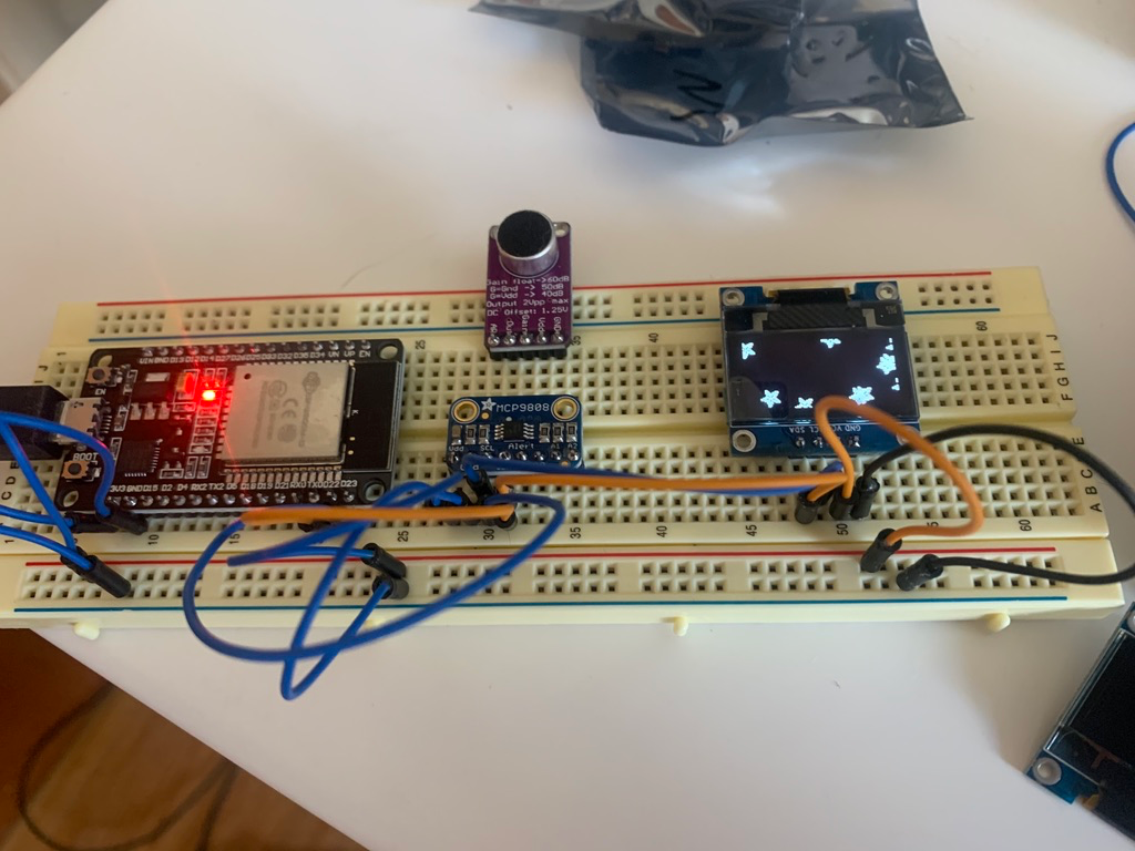
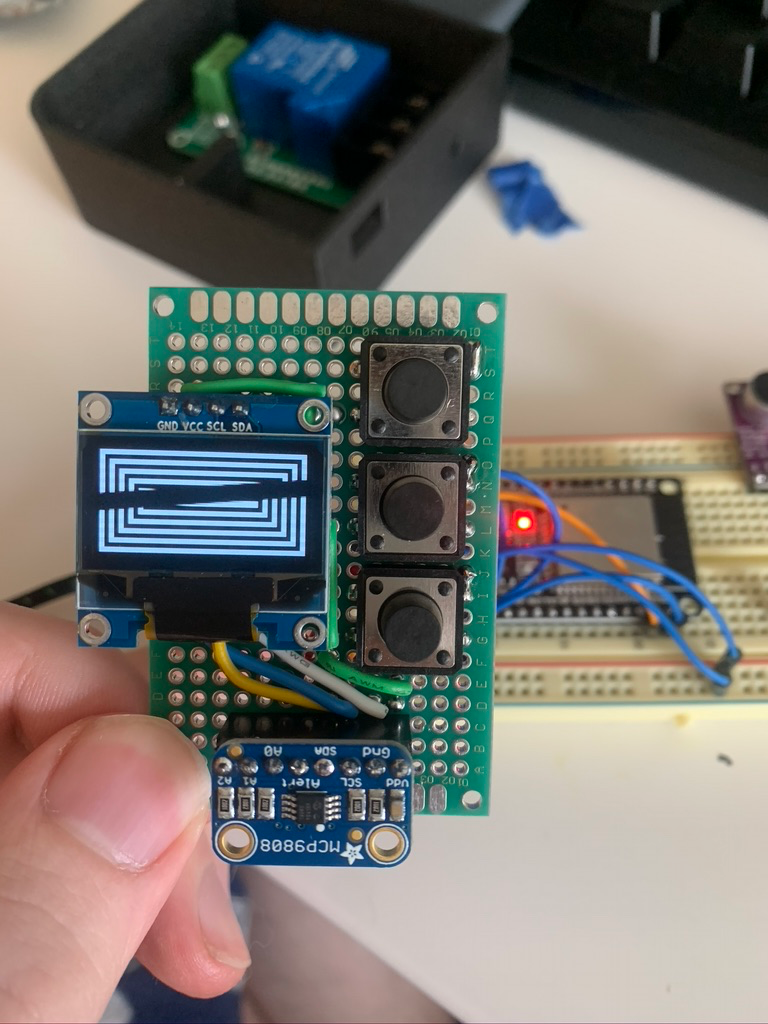
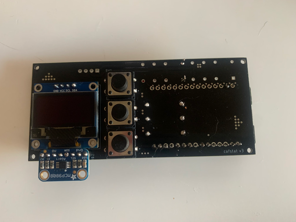
These 3 images represent the stages of any electronics project: Breadboard -> Project Board -> PCB
This project contains 3 different breakout boards and a few through hole components. The brains of the operation are an ESP32 Devkit, there are breakouts for the Thermostat and Screen, and through hold components for the buttons, resistors, and relays.
For this tutorial I will we be using Eagle. It’s got a free tier tool that, and it integrates well into the Autodesk suite. Eagle is free for up to two layer boards, which should be all you need for most electronics projects. The information here will be pretty generally applicable to any tool, although the screenshots will be of eagle specifically.
You can download eagle for free here
A PCB Design contains two main parts, the schematic and the layout. The schematic is an abstract diagram of the connections between components in your project, and the layout is the actual physical layout of those components, and the electrical traces that connect them. The great thing about PCB design software, is that the schematic will be enforced when you are creating the layout, this makes it very straight forward to create the layout after you’ve created the schematic.
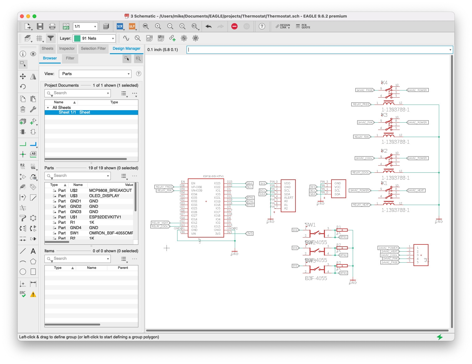
This is the completed schematic for the caffstat project. You can see all of the breakout boards as individual components (red). The connections between them are mostly being managed by net labels to simplify the schematic (more on this later).
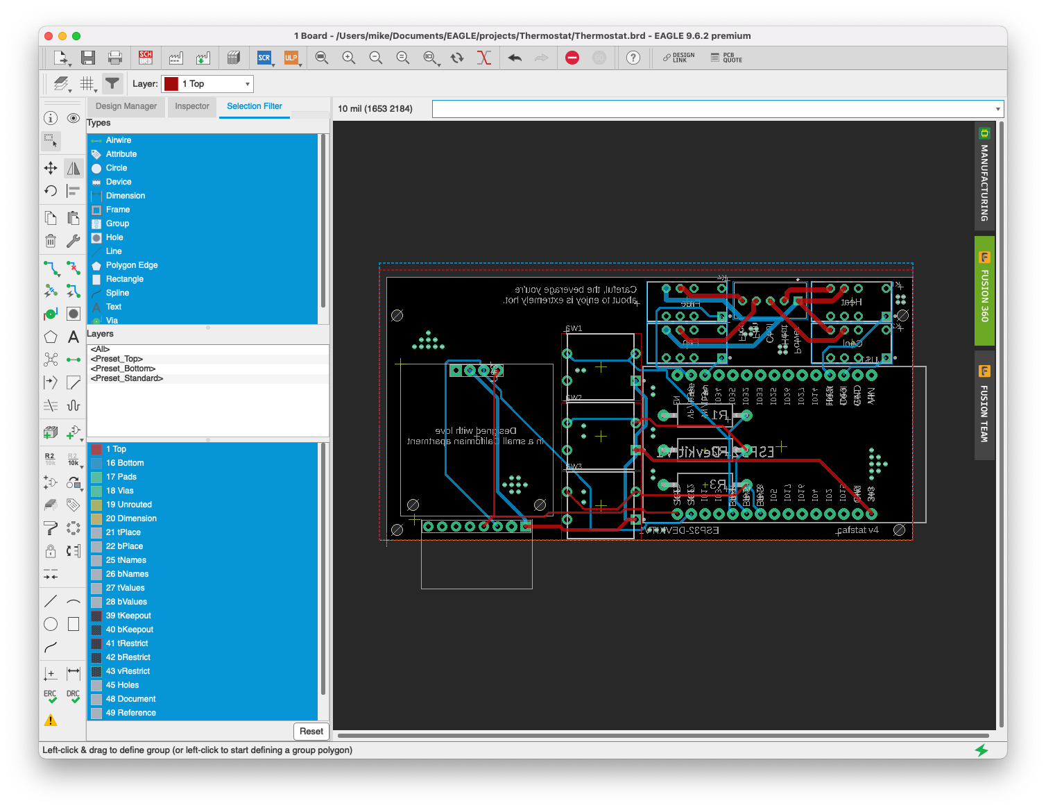
Here is an image of the completed layout. Every component has found a space on the board, and all of the electrical traces have been drawn. Don’t worry if it looks complicated/messy now, when we go step by step it will be very easy to create.
Before you can begin drawing a schematic and layout, you need to find or create models for each and every one of your components. A device model contains both a symbol for part (goes in the schematic) and a footprint of the part (for the layout). I will list out some great resources for finding or creating these here. I can create a full tutorial for creating your own component models if you are interested, let me know at mdl0394@gmail.com
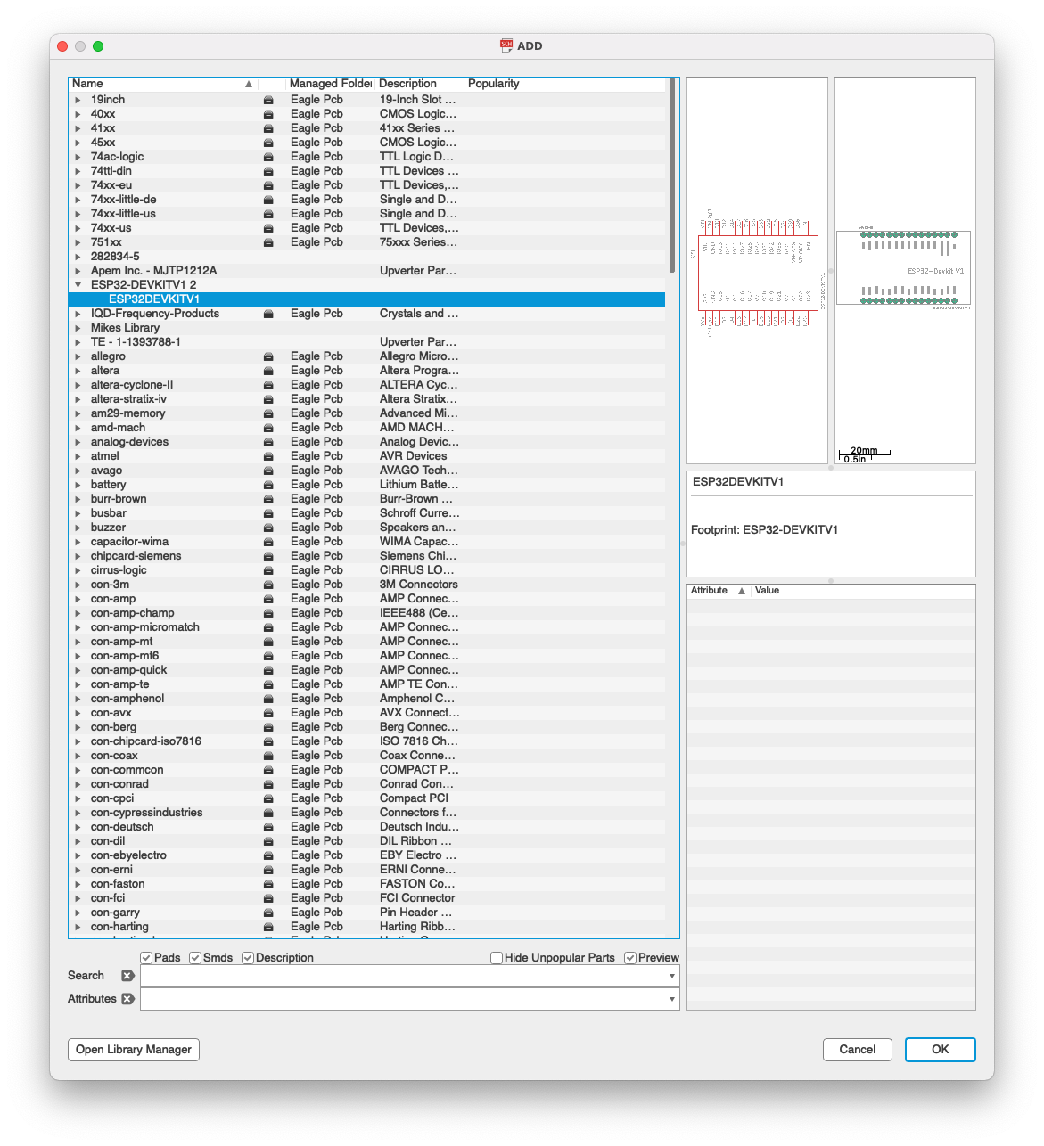
One thing to note is that Eagle comes pre-packaged with a bunch of common components. These are mostly things like standard resistors/capacitors. It’s worth checking the pre-installed library before spending too much time scouring the internet. The easiest way to check the library is to use the “Add Part” button discussed in section 3.2 of this tutorial.
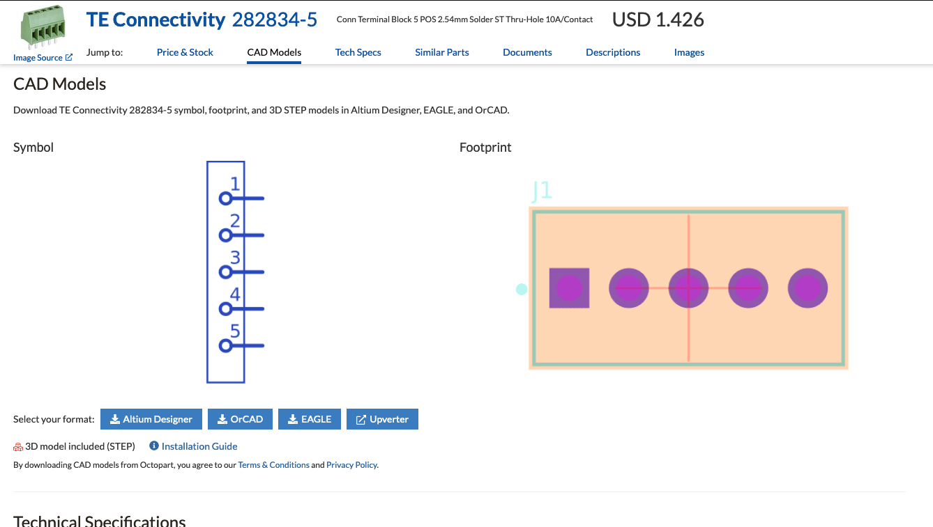
The best tool I have found for looking up components and downloading models is Octopart. Their mission is to provide the best search engine for electronics components. Almost every part can be found in the search engine, I always check here first.
If octopart has the CAD Model for your part, it will appear like this, you want to download the Eagle format, this will download the library that you can install later.
I have also found quite a few schematics by just googling the part. It can often be helpful to try different variations on the name, and include the term “Eagle” or “.lbr” (Eagle library file extension) in your query. If you do find a schematic, make sure you do some measurements (you can do this on the layout of your design) to ensure it matches well with your part (sometimes people upload bad designs, or are modeling something slightly different than yours, you don’t want to order a PCB with bad footprints)
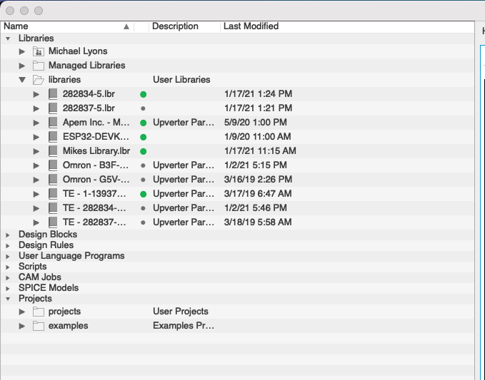
Once you have a library it’s easy to install, drag the Library (.lbr) file into the libraries section of the Eagle Control Panel. Important: after dragging the lbr file, make sure you right click and hit “Use” otherwise you won’t actually be able to add it to your project. Libraries in use will have a green dot next to them
If you fail to find any schematics online (often the case with cheap breakout boards, or with chinese knockoffs) you might have to make your own. It’s not too hard to make your own models, mostly just a little bit tedious. Creating your own models & libraries is a full tutorial in itself, if I get interest I can put that together, for now I will refer you to the resources I used to learn the process.
A good tutorial on how to make custom eagle components can be found here: https://www.build-electronic-circuits.com/eagle-components/
Once you have your components, you can start creating your schematic.
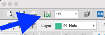
First thing is to make a new Project and new Schematic in eagle. Go into the projects section, right click and hit “New Project”. Then right click and hit “New Schematic”. Once the schematic opens, you also want to create a layout (We’ll use this in Step 4). Do this by hitting the “Generate/Switch to Board” button on the top bar.
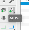
Once you have a schematic you need to put all of your part symbols on. The add part button is on the left bar, clicking this will bring up a dialogue that lets you choose a component. If you don’t see a component you installed here, go back to the control panel and make sure you selected “Use” on the right click menu.
Add all of your components to your schematic. Make sure you give yourself a bunch of room around components to create connections. You should also try to sort the parts in logical groupings, the simpler your schematic, the less likely-hood of bugs.
While placing components there are a few useful tools at your disposal. The Move, Rotate and Copy tools at the top of the left panel are all useful for organizing your schematic. When you want to select an object, the easiest thing to do is to click the + symbol (probably either at the center, or the origin of the part).
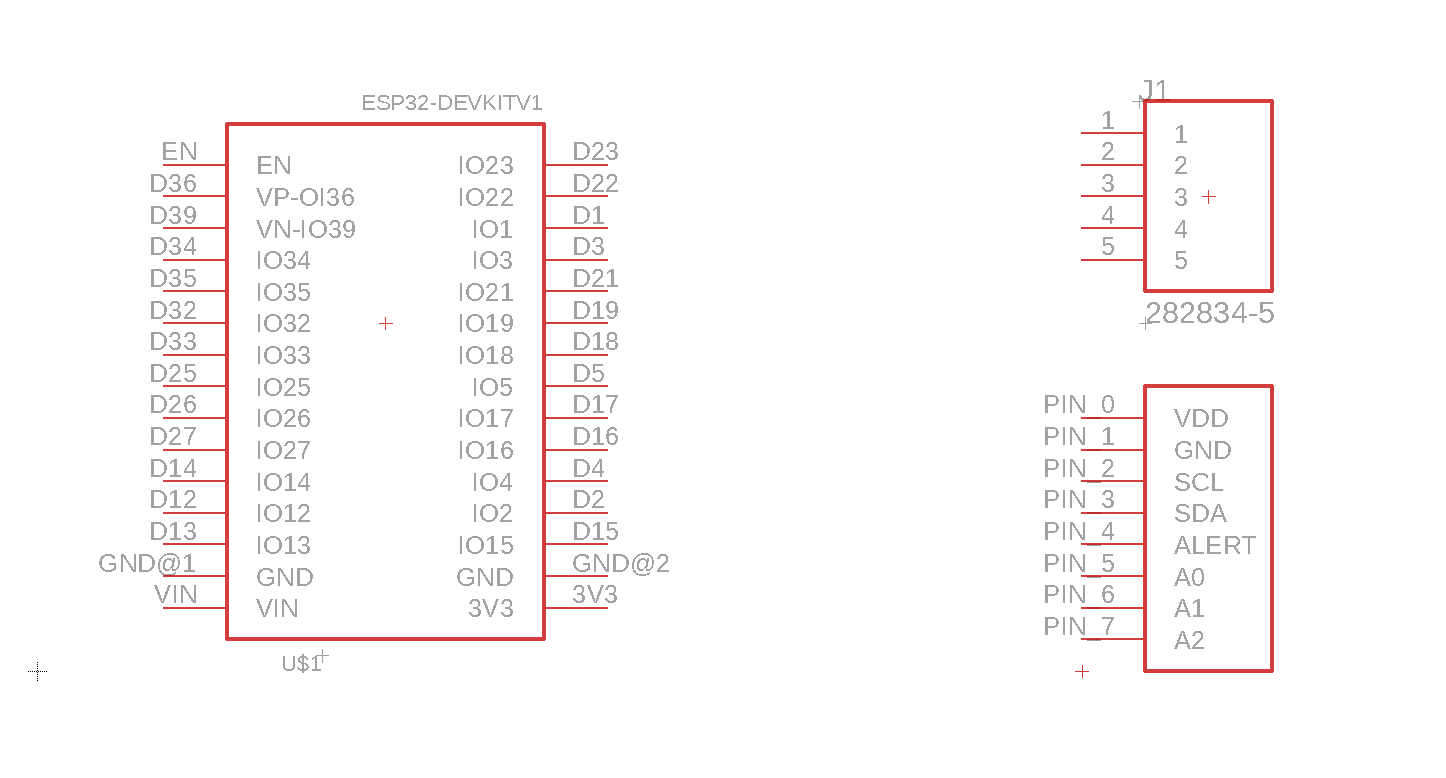
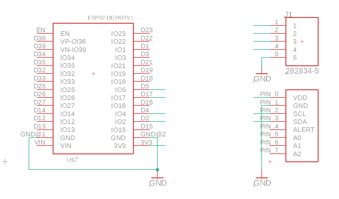
Here is what my schematic looks like after I have placed all of my parts.
The standard for schematics is to use a specialty component to label the shared ground. You can find this by searching “gnd” in the Add Part menu.
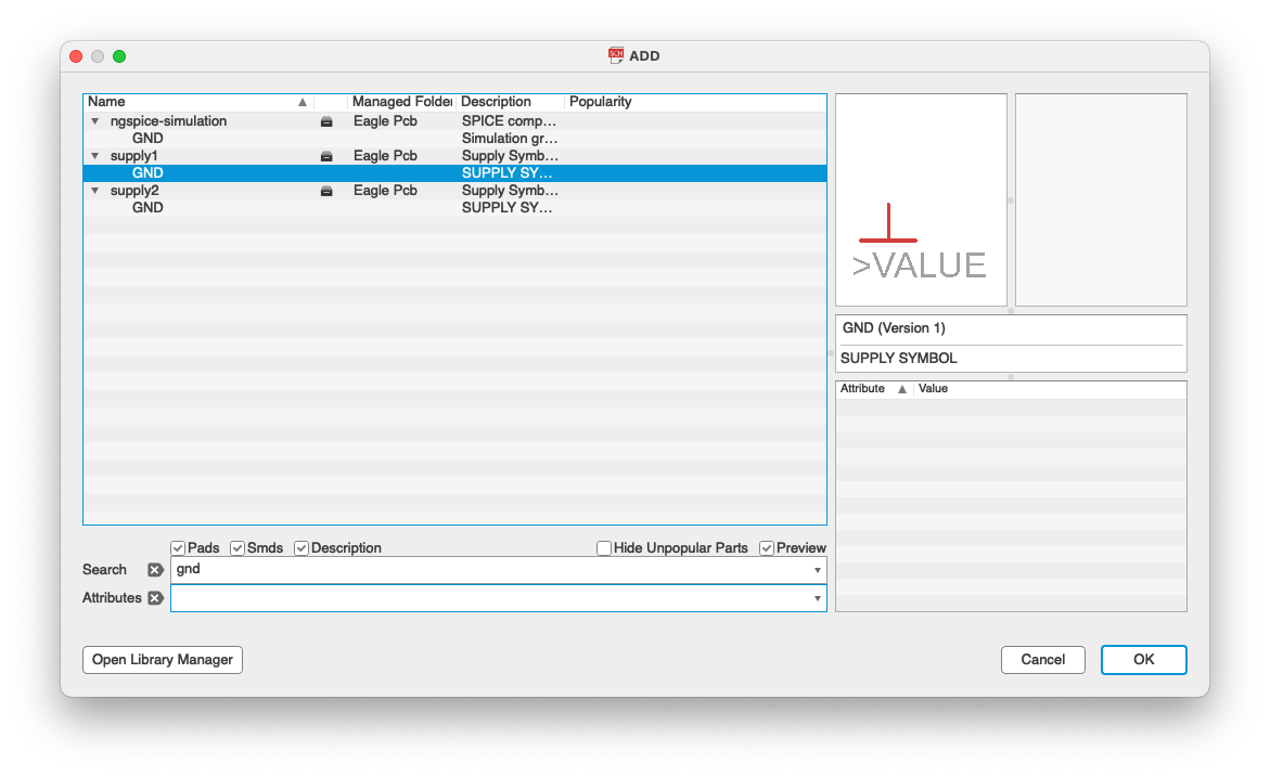
I will usually place one of these per component, just off the bottom of the component, and wire them to the ground pin.
You can directly connect parts together using the “Net” tool (Green line) however with more than a few parts, this will very quickly become unmanageable. Instead of doing that, I will show you how to use labels to cleanly connect parts together. Note that for some components I will not use labels for connections, this makes sense for analog circuits, or things like pull down resistors because they can be logically grouped together.
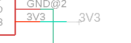
For every node that I want to connect, I will first draw a one or two unit Net. Like so:
Then using the “Name” tool I will name all of the new nets something that makes them easier to keep track of. To name a net, select the tool, then select the green line for the net, a text dialogue should pop up asking you for a name, you can then give the net a unique name, make sure that “Place Label” is checked, and click OK.

Name Tool
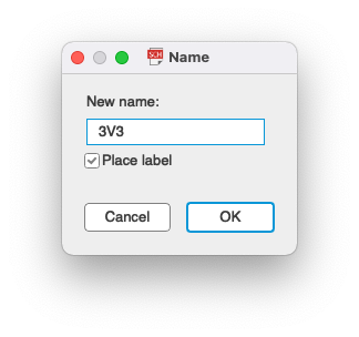
The first label you make probably won’t have the “Xref On” option selected (looks like a little tag symbol on the toolbar). Selecting this will clean up your diagram a bit. I also prefer to set my size to 0.05 so that tags can be neatly stacked on top of each other. You can also use the mirror options to make a left or right side label.

If you want to connect two different nodes together then you should label them the same thing. When you do this Eagle will pop up and ask you if you want to connect the two nets together. Click yes and Eagle will now know that you want those two pins to be on the same net (they will be electrically connected on your layout) .
Once you have all of your components connected properly on the schematic, it’s time to do a final review before moving on to
After wiring all of the components together, I will take a moment to review. Here is the completed schematic diagram for my thermostat motherboard. Before moving on to layout I like to rubber-duck (literally say out loud) the different connections to make sure I didn’t make any stupid mistakes.
In Part 2 I will cover: Board layout, design rules, PCB ordering, and 3d model export. Part 2 will be available in a couple of weeks, subscribe to be notified when it’s posted.